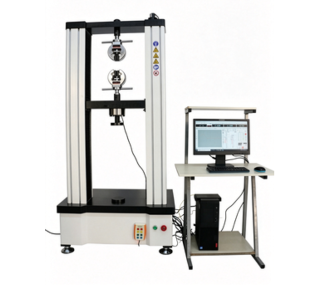
Nano Indenter
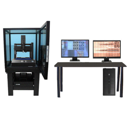


The Nano Indenter / Scratch Tester is a comprehensive micro- and nano-mechanical testing system that integrates four functional modules: nanoindentation, nanoscratch, microindentation, and microscratch. Its modular design allows you to perform indentation, scratch, and friction-wear tests on the same device, ranging from nanoscale to high-load microscale. The instrument provides data on hardness, elastic modulus, creep behavior, elastic-plastic properties, fracture toughness, stress-strain curves, film-substrate adhesion, scratch hardness, friction coefficient, and wear rate, offering a full view of microscopic mechanical properties.
Applications
Measuring hardness and elastic modulus of thin films, coatings, and composite materials
Evaluating microscopic mechanical performance of metals, ceramics, and glass surfaces
Testing wear resistance using nano- and microscratch methods
Analyzing surface performance of MEMS devices and microelectronic materials
Studying adhesion and film-substrate interface bonding of functional coatings
Supporting material development and quality control in industrial and research laboratories
Standards
ISO 14577-1/2/3: Nanohardness and elastic modulus testing of metallic and non-metallic materials
ASTM E2546: Calibration of micro- and nanoindentation instruments
ISO 20502: Nanoscratch testing
ISO 1518: Coating scratch testing
ASTM D7027, D1624, D7187, C171: Scratch testing for coatings and plastics
Technical Specifications
| Module | Parameter | Specification |
|---|---|---|
| Nano Indenter | Max Load | 80 mN / 400 mN / 1800 mN / 4800 mN |
| Min Load | 0.1 mN | |
| Load Resolution | 3 nN | |
| Penetration Depth | 250 μm / 1 mm | |
| Displacement Resolution | 0.0003 nm | |
| Loading Rate | 0.04–12000 mN/min | |
| Nano Scratch | Max Scratch Force | 80 mN / 400 mN / 1800 mN / 4800 mN |
| Scratch Speed | 0.05–600 mm/min | |
| Max Friction Force | 400 mN / 1800 mN | |
| Micro Indenter | Max Load | 40 N / 200 N |
| Min Load | 2 mN / 10 mN | |
| Depth Resolution | 0.01 nm | |
| Penetration Depth | 1 mm | |
| Micro Scratch | Max Load | 40 N / 200 N |
| Max Scratch Length | 50 mm | |
| Max Friction Force | 20 N / 200 N | |
| Precision Positioning Stage | XY Range | 100 mm × 50 mm |
| Z Space | 150 mm | |
| Optical Metallographic Microscope | Magnification | 5X, 10X, 20X, 50X, 1000X (Total 400X–8000X) |
| Atomic Force Microscope (AFM) | Scan Range | 100 μm × 100 μm × 12 μm |
| XY Resolution | 0.1 nm | |
| Z Resolution | 0.02 nm | |
| General | Thermal Drift | <0.05 nm/s (compensated <1 nm) |
| Displacement Accuracy | Grating positioning ≤250 nm | |
| Max Indentation Depth | 1 mm | |
| Max Friction Force | 400 N | |
| Power Supply | AC 220V / 50Hz |
Features
Modular Integrated Design: Combines nano and micro indentation, scratch, and friction-wear tests in one instrument.
International Standard Compliance: Indentation tests conform to ISO 14577 and ASTM E2546; scratch tests conform to ISO 20502, ISO 1518, ASTM D7027, and others.
High-Precision Load System: Closed-loop piezoelectric drive ensures precise and stable load control, superior to traditional cantilever or open-loop systems.
Nanometer-Level Displacement Control: Depth is monitored in real-time by a capacitive sensor, with 0.0003 nm resolution and minimal thermal drift.
High-Accuracy Positioning Stage: Grating-based XY stage ensures repeatability of experiments.
Full-Field Scratch Imaging: Enables optical imaging throughout nanoscratch tests for easier analysis.
Fast Indentation and Scratch Mapping: 100 mapping points can be completed in 5–12 minutes.
Patented Technology: Diamond tip area function calibration ensures accurate and reliable indentation and scratch measurements.
Accessories & Consumables
| No. | Accessory / Consumable | Quantity | Note |
|---|---|---|---|
| 1 | Diamond Indenter Tip | 1 | R-shaped tip, compatible with nano & micro modules |
| 2 | Diamond Scratch Tip | 1 | For nano/micro scratch tests |
| 3 | Constant Load Weights | Several | For micro/high-load calibration |
| 4 | Sample Fixture | 1 set | Fits various sample sizes |
| 5 | Optical Microscope Module | 1 set | For scratch imaging |
| 6 | AFM Probe | 1 set | High-resolution surface scanning |
| 7 | Power Cord | 1 set | AC 220V / 50Hz |
| 8 | Safety Cover | 1 | Provides operational protection |
| 9 | Software Installation Disk | 1 set | For data analysis |
| 10 | Tools & Manual | 1 set | Installation and operation guidance |
Testing Principles
Indentation Testing: Uses high-precision capacitive sensors to monitor the load-depth relationship of steel or diamond tips, providing hardness, elastic modulus, and creep data.
Scratch Testing: Applies controlled load to create scratches, recording friction force, scratch depth, and material damage features, allowing you to determine film-substrate adhesion, scratch hardness, and wear rate.
Multi-Scale Testing: The modular design allows comprehensive mechanical characterization at nano, micro, and high-load scales on the same sample.
Friction & Wear: Measures friction force changes during scratching to evaluate wear resistance and friction coefficient.
Operation Instructions
Confirm sample size and surface condition, then mount it on the precision positioning stage.
Select the test module (nano/micro indentation or scratch) and install the corresponding probe.
Set load, displacement, scratch speed, and number of cycles.
Enable thermal drift compensation to ensure stability during nanoscale tests.
Start the test and observe indentation or scratch morphology using optical microscopy or AFM.
After completion, turn off the instrument, remove the sample and probe, and record experimental data.
Avoid environmental vibrations and high humidity to maintain nanoscale measurement accuracy.
Experimental Procedure
Sample Preparation: Clean, level, and fix the sample on the positioning stage.
Module Selection & Installation: Install the nanoindentation, nanoscratch, microindentation, or microscratch module.
Parameter Setting: Configure load, displacement, scratch length, speed, and cycles.
Thermal Drift Calibration: Activate compensation to ensure precision.
Execute Test: Run indentation or scratch program and record data in real time.
Imaging & Data Analysis: Use optical microscope or AFM imaging and software to analyze mechanical properties.
Completion & Data Saving: Save results, clean samples and probes, and maintain the instrument.
FAQ
1.What is this product?
The Nano Indenter / Scratch Tester, a system for measuring micro- and nano-scale mechanical properties of materials.
2.What is this product used for?
You can measure hardness, elastic modulus, creep, adhesion, scratch resistance, and wear performance of metals, ceramics, coatings, films, and microelectronic devices.
3.Why is this product important?
It allows you to obtain precise mechanical data from nano- to microscale, which is critical for material research, product development, and quality control.
4.What industries is this product suitable for?
You can apply it in coatings, thin films, composite materials, MEMS, electronics, metals, ceramics, plastics, and academic research laboratories.
5.What types of this product are available?
You can choose modules for nanoindentation, nanoscratch, microindentation, and microscratch, with various load capacities to meet different testing needs.
6.What is the difference between nanoindentation and microscratch testing?
Nanoindentation focuses on measuring hardness and elastic modulus at very small scales using controlled load-depth curves (ISO 14577). Microscratch testing evaluates coating adhesion and wear resistance by applying progressive load along a scratch path (ISO 1518, ASTM D7027). The Nano Indenter / Scratch Tester integrates both methods for comprehensive analysis.
7.What factors should be considered when selecting a Nano Indenter / Scratch Tester?
Key factors include load range, displacement resolution, compliance with ISO/ASTM standards, and available test modules. The Nano Indenter / Scratch Tester offers a wide load range from mN to N levels, nanometer resolution, and integrated scratch and indentation functions, making it suitable for both research laboratories and industrial quality control.
Leave Message Get Price